Research and development
A chronological overview of research topics we have worked on jointly with the Faculty of Electrical Engineering and Communication Technologies at the Brno University of Technology.
The main part of our research takes place in modern technologies and design, in cooperation between SMTplus.CZ and the Brno University of Technology, Faculty of Electrical Engineering and Communication Technologies. The company provides manufacturing technology — a pick-and-place machine, wave soldering and more. Students contribute through their bachelor's, master's and doctoral projects.
Electrical interconnection along the z-axis
Together with VUT FEKT we work on layered microsystems. We have solved the connection of PCB modules of arbitrary size to a base substrate via reflow soldering from the side or below. This modular approach makes it possible to:
- partly realise a multi-layer structure on a printed circuit board;
- create a connection that is detachable using classical SMD desoldering methods;
- replace PLCC packages with FLAT-PACK packages (so-called reduction);
- replace part of conventional assembly with surface mounting on an existing PCB.
We also address the problem of connecting a ceramic substrate to an organic FR4 base. Thermo-mechanical stress was simulated, and joint reliability measured and calculated; results were obtained for lead-free SAC solder as well. 3D structures
Silicon solar-cell assembly
Together with SOLARTEC, we explore the assembly of silicon solar cells by a pick-and-place machine. The topic is described in Solar Cell Dice Connecting. The assembly approaches presented allow the use of standard processes — stencil printing, reflow soldering, automated placement — significantly reducing cost.
From 2010, research continued with the Czech Academy of Sciences on assembly of solar chips for concentrators — examining methods and thermo-mechanical reliability on organic (FR4) and ceramic (ALUMINA) substrates.
Reliability of lead-free solder joints
With VUT FEKT we measure the thermo-mechanical reliability of soldered joints in electrotechnics. The work focuses on the reliability of SMT assemblies and on the attachment of semiconductor and solar chips. A dedicated reliability-measurement laboratory was established jointly. Since failures appear as interruptions of varying pulse length, a flip-flop based detection system was developed. See Measurement of thermo-mechanical reliability of soldered joints .
Interconnection of electronic and microelectronic modules (CWC)
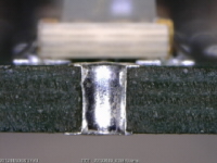
Together with VUT FEKT we address the interconnection of electronic and microelectronic modules via SMD packages. The solution uses the utility model "Electronic assembly of PCB" owned by VUT Brno. Classical chip and cylindrical SMD packages serve as the connecting contacts between the module and the PCB. Free translation: New connection of electronic modules.
The principle CWC (Connection With cylindrical and Chip Components) is shown in the figures. The electronic or microelectronic module (1) is connected to the printed board (2) through the leads of classical SMD packages (chip or cylindrical; 3, 4).
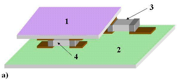
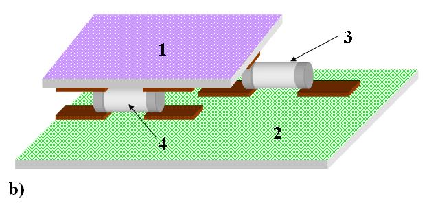
Advantages of the connection:
- standard pick-and-place machines with common feeders can be used;
- if packages are sufficiently tall, electronic components can be placed on the underside of the module as well;
- the relatively large lead height substantially reduces thermo-mechanical stress on the soldered joint, which can lead to increased system reliability.
In 2011 the joint project with VUT Brno FEKT — TIP project FR-TI1/072 "Application of modern assembly technologies and materials in the electrotechnical industry", announced by the Ministry of Industry and Trade of the Czech Republic — concluded. INFO
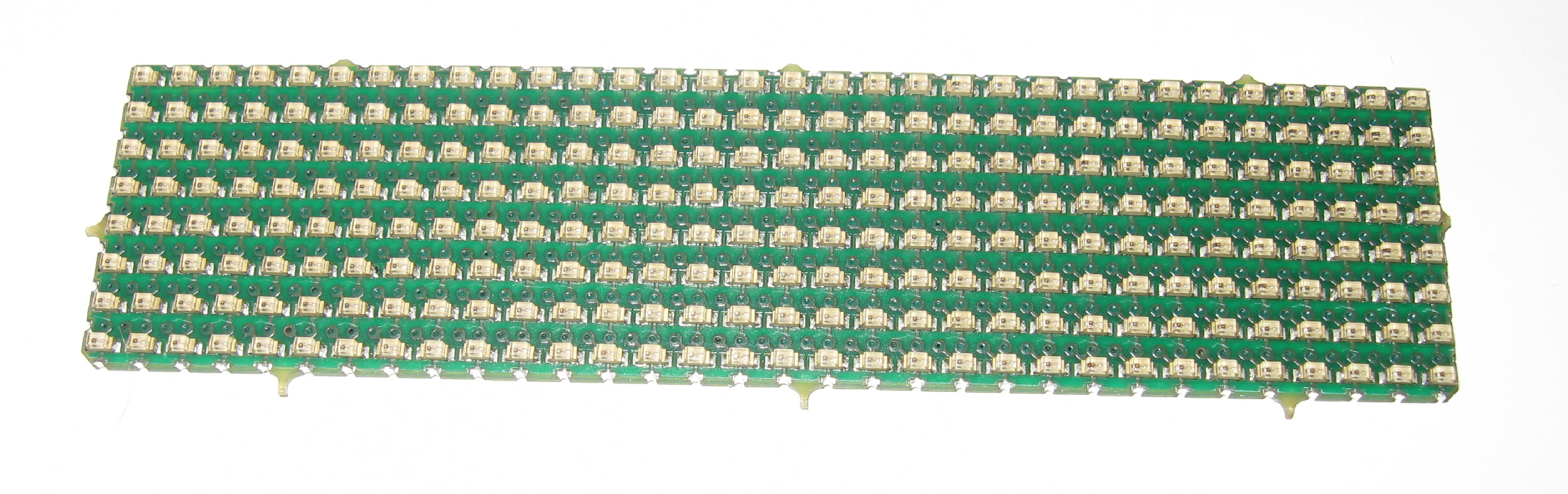
Within the project, modules for layered 3D interconnection were designed, along with a matrix display of 256 LEDs in 0603 SMD packages. The display is connected to the base board by edge interconnection.
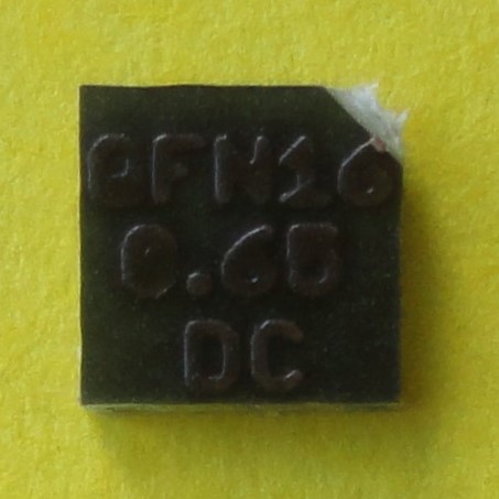
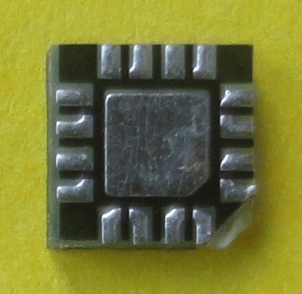
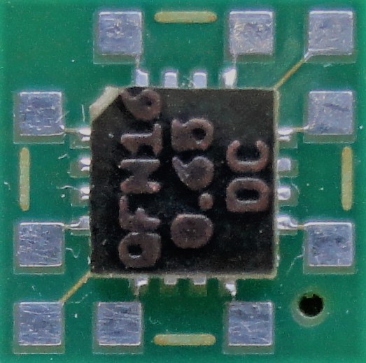
QFN package assembly and soldering training
Within research, we designed and produced a test QFN16 package and a test PCB with a daisy-chain pattern for ohmic verification. The setup allows the correct soldering of the test package to be checked with a multimeter. Since 2020, the solution has been used for QFN soldering training in our practical SMT courses.
No significant research took place between 2019 and 2022. Reported by Ass. Prof. Ing. Josef Šandera, Ph.D. — updated 09/2023